Switching to VLSI from IT Services: A Career Guide for 3-5 Year Engineers (India 2026)
TL;DR. Switching to VLSI from IT services is one of the highest-leverage career moves available to a 3-5 year Indian engineer in 2026 — but only if you pick the right specialisation for your existing skills and commit to 12 months of focused learning. Verification, RTL design, and CAD/EDA are the natural bridges. Physical design is hard without fundamentals. Expect a short-term pay cut, break-even by month 18, and 2-3x your current CTC by year 3. This is the plan.
I've spent 12 years in the semiconductor industry, mostly at NVIDIA and Samsung as an SoC architect. In the last three years, I've mentored eight engineers making this exact transition — from IT services backgrounds into VLSI. Six made it. Two didn't. The difference wasn't intelligence. It was fit, strategy, and honest self-assessment about where they were starting from.
Let me walk you through what actually works.
Why this move makes sense in 2026
Four structural factors are converging in India's favor right now:
- The India Semiconductor Mission has committed over $10 billion to domestic fab buildout. Tata Dholera, Tata OSAT Assam, Kaynes Sanand, and the Micron Sanand assembly plant are all under construction or ramping. Every fab drives design-service demand 10x its fab headcount. See our tracker on India's semiconductor fabs coming in 2026-2028.
- Talent shortage is severe. India produces roughly 300,000 ECE/EEE graduates per year but only 3-5% of applicants clear VLSI product-company hiring bars. The gap is a crisis for the industry and an opportunity for you.
- IT services pay has stagnated. The 12% annual raise at TCS or Wipro is gone. Most 3-5 year engineers in Indian IT services are making 6-11 LPA with slow-moving ceilings. VLSI pay at the same experience level is 15-40 LPA.
- AI chip demand is compounding. Every foundational model being trained requires silicon. NVIDIA, AMD, and dozens of AI-chip startups are hiring aggressively in India. Current verification and PD openings on our job board confirm this.
The tailwind is real. It rewards engineers who move now, not in 2028.
The honest reality check
Before the roadmap, the caveats I give every mentee:
- You will take a short-term pay cut. Most make the jump at ~90-100% of their current CTC. Expect 12-18 months before you catch up, then a steep curve.
- The learning curve is real. Digital design, SystemVerilog, UVM, and one EDA tool take 9-12 months of consistent effort alongside a full-time job. Not weekend-warrior effort. Daily effort.
- Not every software background maps cleanly. A backend Java developer has a better path than a frontend React developer. A systems/C/kernel engineer has an even better path. Be honest about your starting point.
- Your IT services title gets discounted. "Senior Software Engineer, TCS" reads as roughly "2-3 year junior VLSI engineer" at product companies. Your 5 years of Java don't transfer as 5 years of semiconductor experience. This is frustrating but real.
- An M.Tech is usually not the answer. A 2-year M.Tech from most Indian colleges costs you 2 years of income and adds limited practical skill. Exceptions: IIT, IISC, and a few NITs for research-oriented roles. For everyone else, focused self-study plus a service-company VLSI entry is faster.
If you're still in after reading those, you have the right temperament for the move. Let's plan it.
Which VLSI specialisation fits which software background
This is the decision that determines whether you succeed. Pick wrong and you'll fight your own instincts for 3 years.

Pick the row closest to your current role, then read the filled circles as your top specialization candidates.
If you're a backend / Java / Python engineer
Best fit: Verification. Verification is about writing testbenches — structured, object-oriented code in SystemVerilog and UVM. Your OOP instincts, testing discipline, and debugging experience transfer directly. The domain shift is learning digital design fundamentals and simulation semantics.
Second-best: RTL Design. If you like writing code that describes behavior, RTL is coding too — just in a hardware description language. Be ready for the mental shift from sequential execution to concurrent signals.
If you're a systems / C / kernel / embedded engineer
Best fit: DFT or CAD/EDA. DFT involves scan chains, ATPG, and test vector generation — close to your low-level systems intuition. CAD/EDA involves tool development and flow automation — directly leverages your scripting and systems programming depth.
Second-best: RTL or Verification. Systems engineers adapt well to both. If you've written firmware, you already think like a hardware engineer.
If you're a front-end / web / full-stack engineer
Honest answer: this is the hardest transition. The paradigm shift from request-response web development to clock-driven hardware is large. Not impossible — I've seen it work — but you'll be re-learning fundamentals almost from scratch. Expect 15-18 months of prep, not 12.
If you're committed: start with Verification. Testbench work uses software patterns you already know. Once inside the industry, you can pivot to RTL or PD if the work interests you more.
If you're a data scientist / ML engineer
Best fit: Hardware-software co-design or AI accelerator teams. Companies building AI chips (NVIDIA, AMD, Cerebras, Groq, domestic startups) need engineers who understand both ML workloads and silicon. You won't start in deep PD or RTL, but ML-aware verification and architecture roles are growing fast.
If you're an IT services engineer doing testing / QA
Best fit: Verification. Your testing mindset is the closest natural fit in IT services. The gap is technical: SystemVerilog, UVM, and digital design fundamentals. Your QA discipline is already more aligned with verification than most junior candidates from product-company software roles.
The skill gap, quantified
Here's what you need to add, organized by priority:
Must-have (months 1-6)
- Digital design fundamentals. Combinational logic, sequential logic, FSMs, timing (setup/hold), CDC, metastability. Read Morris Mano or Digital Design by John Wakerly cover-to-cover.
- SystemVerilog. Classes, randomization, constraints, interfaces. For verification, this is your primary language for the next decade.
- One EDA tool. For verification: Synopsys VCS or Cadence Xcelium. For RTL: any simulator plus Design Compiler for synthesis awareness. For PD: ICC2 or Innovus. Get hands-on. Tutorials are not enough.
Should-have (months 6-12)
- UVM (for verification track). The industry-standard methodology. Read the Accellera UVM 1.2 reference manual. Build a testbench from scratch for a non-trivial block.
- Protocols. AXI, APB, PCIe basics. Know them well enough to verify them.
- GitHub portfolio. Public projects that prove you can do the work. A clean UVM testbench for a FIFO or a full synthesized RISC-V core signals intent and capability.
Nice-to-have (months 12+)
- Scripting for EDA flows (Tcl, Perl, Python) — helps at every specialisation
- Low-power design concepts (UPF, power gating)
- Formal verification basics (for PD and verification roles at senior companies)
The 12-month roadmap
Months 1-3: Foundation
Read one digital design textbook. Work through every exercise. Build a simple project — an FSM controller, a traffic light, or a UART — in Verilog or SystemVerilog.
Set up a working EDA environment at home. Use open-source tools if you don't have vendor access: Icarus Verilog for simulation, Yosys for synthesis, OpenROAD for PD experimentation.
Decide your specialisation track based on the fit analysis above. Stick with it. Pivoting at month 4 resets your progress.
Months 4-6: Specialisation depth
Start building specialisation-specific skills:
- Verification: Learn SystemVerilog advanced features, start UVM via the Accellera tutorials and Ray Salemi's book
- RTL: Build increasingly complex designs — a pipelined processor, a DMA controller, an AXI-compliant bus
- DFT: Learn scan insertion, ATPG, and test compression basics via academic resources
- CAD/EDA: Contribute to open-source EDA projects (OpenROAD, Verilator, Yosys)
Publish everything on GitHub. Write README files that explain decisions, not just what the code does.
Months 7-9: Interview prep + applications
Start interviewing at service companies doing VLSI work — Wipro VLSI, L&T Technology Services, Tata Elxsi, HCL, KPIT. These are your entry doors.
Pay range for first-time VLSI hires with IT services background: 8-14 LPA. Lower than your IT services salary? Maybe. Lower than product-company entry? Definitely. But this is the bridge, not the destination.
Prepare specialisation-specific interview content. For verification, see our verification interview guide. For physical design, see our PD interview guide.
Months 10-12: Land and learn
Target a role with real project work — tapeout, real silicon, real customer deliverables. Avoid pure-support roles (documentation, test running). You need production chip experience to be valuable to a product company.
Once in, spend the first 12 months absorbing. Pair with senior engineers. Learn the methodology. Build your tapeout story. By month 18-24 from the switch, you're ready for the product-company jump.
Companies that hire career-switchers
Not every company takes IT services transitions seriously. These ones do:
Service companies (entry bridge)
- Wipro VLSI — Bangalore. Large hiring volume. Structured training programs.
- L&T Technology Services (LTTS) — Multiple locations. Strong in automotive and aerospace semis.
- Tata Elxsi — Bangalore, Chennai. Growing VLSI practice.
- HCL Technologies — Multiple. Has a chip design business unit separate from its mainstream IT services.
- KPIT — Pune. Automotive chip design focus.
- Sankalp Semiconductor (Arm) — Bangalore. Acquired by Arm, good entry point for ARM-ecosystem work.
Target entry CTC: 8-14 LPA for career-switchers. Real tapeout exposure after 18-24 months.
Product companies (year 2-3 target)
After 18-24 months at a service company with real project experience, you're competitive for:
- Cadence Design Systems, Synopsys — EDA companies. Lateral-friendly. Good mid-career entry.
- Intel, Qualcomm, Broadcom — Top-tier product companies. Hire laterals with 2+ years of real design experience.
- Samsung Semiconductor — Strong verification and PD teams. Lateral-friendly for candidates with specialisation depth.
- NVIDIA, AMD — Highly selective. Realistic target at year 3+.
Target product-company CTC after 3 years in VLSI: 25-45 LPA. That's 2-3x your current IT services package.
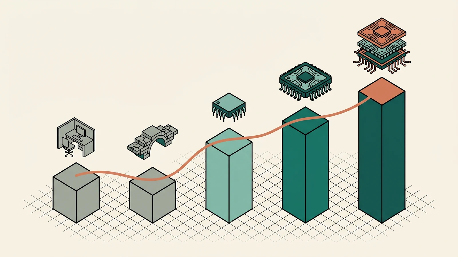
Salary expectations — the honest numbers
Year 0 (current IT services): 6-11 LPA as a 3-5 year engineer at TCS, Wipro, Infosys, Cognizant, Accenture.
Year 1 (VLSI service company entry): 8-14 LPA. Lateral move or slight bump. Short-term pain.
Year 2 (VLSI service company, with project experience): 12-18 LPA. Real tapeout exposure unlocks better opportunities.
Year 3 (VLSI product company): 20-35 LPA. Cadence, Synopsys, Intel, Qualcomm all become realistic.
Year 4-5 (VLSI product company, specialised): 30-50+ LPA. Senior individual contributor at top-tier company. For full breakdown by specialisation and level, see our VLSI engineer salary guide 2026.
Break-even from IT services peak: around month 18-24. Upside from year 3 onwards: 2-4x your current trajectory.
How to position your IT services experience in an interview
The framing matters. Done right, your IT services background is a mark of discipline, teamwork, and enterprise-scale thinking. Done wrong, it reads as "this person didn't make product-company cut."
Say this:
- "Five years of delivering production software at scale under strict SLAs."
- "Led debugging of a distributed system failure in production — I'm bringing that debug discipline to hardware verification."
- "Worked across 40+ engineers on a single release — I understand how big teams coordinate."
- "Self-taught SystemVerilog and built this public UVM testbench for a FIFO block — here's the GitHub link."
Don't say this:
- "I want a career change." (Vague.)
- "I want to do hardware because it's more exciting." (Sounds naive.)
- "VLSI pays more." (Even if true, never lead with it.)
Lead with specifics: what you built in your own time, what you taught yourself, what you want to learn next.
Two red flags to avoid
The offline VLSI training trap
Many coaching institutes in Bangalore, Hyderabad, and Chennai offer 3-6 month VLSI training programs for career-switchers. Costs 1-3 lakhs. The honest reality: most of these programs teach tool operation, not engineering fundamentals. You come out knowing how to click buttons in Innovus, not why.
The good ones exist — Maven Silicon and VLSI Guru are generally solid — but even these are supplementary. They are not a substitute for self-study and a GitHub portfolio. A hiring manager values a good public project over any certificate.
The "just do an M.Tech" trap
2 years out of the workforce, 10-15 lakhs tuition, and most Indian M.Tech programs in VLSI teach outdated methodologies. Exception: IIT, IISC, top NIT, or a specialised program at BITS. For these, the ROI can work. For a tier-3 M.Tech, you're worse off than if you'd spent that time self-studying with a service-company job.
The bottom line
If you're a 3-5 year engineer at an Indian IT services company with systems thinking, debug discipline, and a willingness to commit 12-18 months to focused learning, this move is one of the best career decisions available to you in 2026.
The industry needs you. The ceiling is higher. The work is more intellectually dense. And if you execute this roadmap, your year-3 compensation will be 2-3x your current trajectory.
Start this week. Pick your specialisation. Read the first textbook. Browse current VLSI openings to understand the market. Match your GitHub projects to what product companies are asking for.
Eighteen months from now, you'll thank your current self for making this decision.
Related reading
- VLSI engineer salary in India 2026: the complete guide
- VLSI Verification Engineer Interview Guide 2026
- Physical Design Interview Questions: The Complete Guide for India 2026
- Top 10 semiconductor companies hiring VLSI engineers in India
- India's semiconductor revolution: every fab and OSAT plant coming in 2026-2028
Frequently asked questions
Can I switch from TCS, Wipro or Infosys to a VLSI career in India in 2026?
Yes, and it is one of the highest-leverage career moves available to a 3-5 year engineer right now. The right path is: self-study digital design and SystemVerilog for 6-9 months, build a GitHub portfolio, then enter a VLSI service company (Wipro VLSI, LTTS, Tata Elxsi, HCL, KPIT, Sankalp/Arm) as your bridge. From there, target product companies at year 2-3. Expect a short-term pay cut and 12-18 months to break even, then 2-3x compensation by year 3.
Which VLSI specialisation is easiest for a software engineer to switch to?
Verification is the best fit for most software engineers. The testbench work is object-oriented code in SystemVerilog with extensive testing discipline — directly leveraging OOP, debugging, and QA skills. Your second option is RTL design if you enjoy describing behavior through code. Physical design is the hardest path without digital fundamentals; avoid it as a first move. For systems/C/kernel engineers, DFT and CAD/EDA are also strong fits.
Do I need an M.Tech to switch from IT services to VLSI?
Usually no. Unless you're targeting IIT, IISC or a top NIT M.Tech program (which do carry real brand value), a 2-year tier-3 M.Tech costs you income and adds limited practical skill versus focused self-study plus a service-company entry. Hiring managers at product companies value GitHub projects and real tapeout experience over an M.Tech certificate from most Indian colleges.
What salary can I expect in year 1 after switching from IT services to VLSI?
Realistically 8-14 LPA at a VLSI service company (Wipro VLSI, LTTS, Tata Elxsi, HCL, KPIT) for a 3-5 year IT services engineer. This is typically at or slightly below your current IT services CTC. The economics are year-2 onwards: 12-18 LPA with project experience, then 20-35 LPA at a product company by year 3. The curve is steep once you're in the industry.
How long does it take to prepare before applying to VLSI companies?
Nine to twelve months of consistent daily effort alongside your current job. Months 1-3: digital design fundamentals and SystemVerilog basics. Months 4-6: specialisation depth (UVM for verification, advanced RTL for RTL track, etc.) and GitHub portfolio. Months 7-9: interview prep and applications. Front-end/web engineers should budget 15-18 months instead. Shortcuts exist for systems engineers; they rarely exist for web engineers.
Are offline VLSI training institutes in Bangalore or Hyderabad worth it?
Some are, most aren't. Maven Silicon and VLSI Guru have generally good reputations. Most others teach tool operation (clicking through Innovus or VCS) rather than engineering fundamentals. These programs are at best supplementary to self-study and a GitHub portfolio. A hiring manager values a solid public project over any training certificate. Spend time and money there only after your fundamentals are solid.