Physical Design Interview Questions: The Complete Guide for India (2026)
TL;DR. Physical design interviews in India test five things in order: flow fluency, timing closure depth, tool command, debug instinct on a real block, and a project story with specific metrics. Most 3-5 year candidates nail the flow questions and flame out on timing closure. This guide gives you the 40 real questions I've both asked and been asked in the last three years, plus the six-week prep plan I give every engineer I mentor.
I've spent 8 years in physical design across Intel and Cadence and have interviewed over 200 candidates. PD has strong demand in India — currently around 140 active physical design openings on our PD job board — but the bar is higher than verification. Fewer PD engineers exist. Companies are pickier. And the difference between a 12 LPA and a 35 LPA offer often comes down to how you answer four or five specific timing closure questions.
Let me walk you through exactly what you'll face.
What physical design interviewers actually test
After reviewing debrief notes across dozens of hiring loops, the weight is consistent:
- PnR flow fluency (25%). Synthesis to signoff. Not just naming the steps — explaining why each exists, what can fail at each, and what the handoff between steps looks like.
- Timing closure depth (25%). This is the differentiator. Setup, hold, clock skew, OCV, CPPR, useful skew. Everything interviewers want to know whether you've actually closed timing on a block or just run the tool.
- Tool command (15%). ICC2 or Innovus, depending on which tool your target company uses. Command-level fluency matters.
- Debug and problem decomposition (20%). Given a congestion issue, a timing violation you can't close, or a DRC explosion — where do you look first?
- Project story (15%). Specifics: the block, the process node, your contribution, the metrics you hit.
The candidates who get offers at product companies have run a full flow themselves at least once. The ones who get stuck at service companies usually haven't.

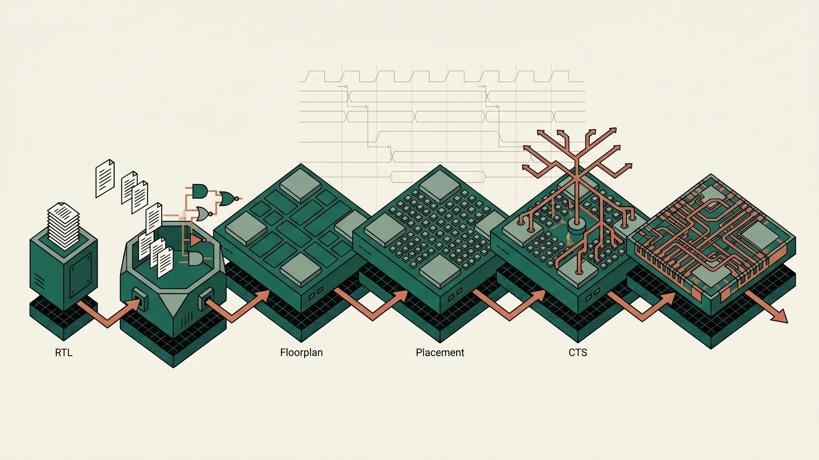
The 7-stage flow every PD interview Round 2 walks through — and the specific failures interviewers ask about at each stage.
The typical interview structure
Round 1: Technical screen (45-60 min)
Fundamentals check. Often with a PD senior engineer.
- Digital design — setup time, hold time, metastability, CDC
- Basics of synthesis — what the synthesizer does, what constraints it needs
- PnR flow overview — floorplan, placement, CTS, routing, signoff
- A timing question: "Given this path, calculate the slack."
Freshers and mid-level both get this round. Differentiation is the depth of answers, not the breadth of questions.
Round 2: PnR flow deep dive (60-90 min)
You'll walk through the full flow. Expect whiteboarding.
- "Draw a floorplan for a block with 3 hard macros and 2 clock domains. Where do you place the macros?"
- "Your placement is done and you see 40% congestion in one region. What's your move?"
- "Walk me through CTS — from reading the clock spec to checking skew after optimization."
- "Your design is routed but you have setup failures. What are the first three things you try?"
Round 3: Timing closure (60-90 min)
This is the round that determines your offer level.
- "Explain OCV vs. AOCV vs. POCV."
- "You have a setup failure on a multi-cycle path. The SDC says it's a 2-cycle path but PrimeTime reports single-cycle slack. What's wrong?"
- "When do you use useful skew? When do you avoid it?"
- "Your block has 200 setup violations after routing. You can't change the RTL. What are your options?"
Round 4: Project deep dive + managerial (60 min)
Pick a block. Process node. Your contribution. Specific numbers. The ECO you ran. The timing closure strategy. Tool flow you followed.
Killer question: "Tell me about a block that didn't meet timing and what you did." Have a real answer.
Round 5: HR and offer (30 min)
CTC, location, team. Technical decision is made by now.
40 real physical design interview questions, with answers
Synthesis and constraints (1-5)
1. What's the difference between clock gating and clock enable?
Clock enable uses a mux at each register to hold state when inactive — power is still consumed by toggling clock pin. Clock gating blocks the clock upstream via an ICG cell, preventing toggles on the register. Clock gating saves significantly more dynamic power but adds insertion delay and can cause timing issues in CTS. Production SoCs use both strategically.
2. What does the set_multicycle_path constraint do, and what's a common mistake with it?
It tells the timing tool to allow more than one clock cycle between launch and capture. The common mistake is setting multicycle for setup without also adjusting hold — causing hold violations the tool doesn't catch. Always set both setup and hold multicycle, and understand which edge you're referencing (-start or -end).
3. Why do we need set_input_delay and set_output_delay?
They define the timing context at block boundaries — how much delay exists on inputs coming in (relative to the clock) and how much delay is allowed on outputs going out. Without them, the tool has no reference for I/O timing and your block will have unrealistic slack numbers at boundaries.
4. What's a false path, and when should you NOT declare one?
A false path is a physical connection the design never exercises functionally — common in CDC paths or reset synchronizers. Don't declare false paths on CDC signals without proper synchronizers in place; otherwise you're hiding real bugs. Also never use false_path when multicycle would be more accurate.
5. Explain the difference between ideal clock and propagated clock modes.
In ideal mode, the tool assumes the clock has zero skew and is already balanced — used during synthesis and early placement. Propagated mode uses actual clock tree delays — used after CTS. Running timing analysis in the wrong mode will give you wrong slack numbers.
Floorplanning and placement (6-11)
6. What drives floorplan aspect ratio?
Block utilization target, macro placement feasibility, and package pinout constraints. Too square and you waste area; too rectangular and routing becomes congested. Typical blocks land between 0.8 and 1.25 aspect ratio. For high-utilization blocks, closer to square reduces congestion.
7. How do you decide where to place hard macros?
Against the boundary if possible — frees up core area for standard cells. Orient pins toward where nets connect most (typically the datapath). Keep macros with shared signals close together. Leave channels between adjacent macros if routing density demands it. Never let macros overlap with pre-placed power straps.
8. What's a halo around a macro and why does it matter?
A physical keepout region around a hard macro where standard cells can't be placed. Prevents placement tool from stuffing cells into areas that would block routing to the macro pins. Typical halo is 10-15 microns for memory macros. Too small = congestion; too large = area waste.
9. Your placement shows 45% congestion in one region. What are your moves?
Reduce utilization locally via placement blockages. Check if a large macro is blocking channels — may need to re-orient. Check cell density; if high-fanout cells cluster, spread them with placement density constraints. If RTL allows, replicate high-fanout drivers. Last resort: re-floorplan.
10. What's cell padding and when do you use it?
Adds space around specific cells during placement to prevent pin-access issues. Common for flops and MUXes in high-density designs. Too much padding = area bloat; too little = unroutable nets. A 1-2 site pad on flops is standard for 7nm and below.
11. When would you pre-place cells instead of letting the tool decide?
Critical-path cells where placement quality directly drives timing. Large clock buffers at strategic points before CTS. Cells driving high-capacitance long nets. If a block has a known timing-critical launch flop to capture flop pair, pre-placing near each other is cheap timing insurance.
Clock tree synthesis (12-15)
12. What's the difference between clock skew and jitter?
Skew is the static spatial difference in clock arrival between sinks (difference between launch and capture). Jitter is the cycle-to-cycle timing variation on the clock itself. Skew is a layout-controlled problem. Jitter is a PLL/clock source problem.
13. How do you decide the target clock skew?
Zero skew is ideal in theory, but real trees have insertion delay variation. Target 50-100 ps skew budget for most designs. For high-frequency blocks (>2 GHz), tighter. For low-speed control blocks, you can relax. Too tight and CTS will over-buffer, burning power.
14. What's useful skew and when do you apply it?
Intentionally unbalancing the clock tree so launch flops receive the clock earlier or later, effectively borrowing time across a path. Use it when setup-critical paths can't close timing any other way — but it creates hold violations elsewhere, so apply conservatively and verify hold after.
15. After CTS your max transition on the clock network is failing. What's wrong?
Weak buffers in high-fanout sections, too-long nets between buffers, or a load imbalance at a specific branch. Fix: upsize buffers in the failing region, add intermediate buffers to break long nets, or re-balance the tree.
Routing and DRC (16-18)
16. What's the difference between global routing and detailed routing?
Global routing plans the rough path of each net through routing channels, ignoring exact track assignment. Detailed routing assigns actual metal tracks and checks DRC. Global routing congestion estimates are the main input to placement optimization.
17. You have a DRC explosion after detailed routing. How do you debug?
Look at DRC by layer first — is it one layer or all? Check if certain cells cluster in failing regions (poorly characterized cells). Look for spacing violations near memory macros (halo may be too small). Check for antenna violations from long routes — may need diode insertion or wire hopping.
18. Why do we need metal fill post-routing?
Maintain metal density uniformity for CMP (chemical-mechanical polishing) planarity. Without fill, low-density regions cause dishing during wafer processing. Fill is required for every metal layer and must pass foundry density rules.
Timing closure (19-26)
19. Explain OCV, AOCV, and POCV.
OCV (on-chip variation) applies a flat derating to path delays for uncertainty. AOCV (advanced) derates based on path depth — shallower paths get less derating because statistical averaging is stronger at depth. POCV (parametric) models each cell's variation statistically, giving tighter estimates. Modern 7nm and below use POCV; older nodes used AOCV.
20. What's CPPR and why does it matter?
Clock path pessimism removal. The timing tool applies OCV derating to both launch and capture paths, but if they share common clock tree segments, that shared portion cancels — it can't have OCV on both sides. CPPR removes the false pessimism. Without CPPR, your slack numbers are overly conservative and you'll over-fix.
21. Your block has 200 setup failures at post-route. RTL is frozen. Walk through your closure plan.
Sort violations by severity and group. For the worst: check if path has logic that can be restructured at ECO (buffer insertion, gate sizing). For medium: useful skew via CTS ECO. For low: driver upsizing and delay cells on capture. In parallel: check SI and crosstalk — many "logic" failures are actually crosstalk issues. Re-run timing with ideal crosstalk to isolate.
22. How do you fix a hold violation?
Insert delay buffers on the launch side of the path. Prefer low-drive-strength cells. Never fix hold by reducing setup slack more than necessary — it's tempting but costs area. Check whether useful skew was applied upstream creating hold; you may need to reverse it.
23. What's the difference between pessimistic and optimistic timing analysis?
Pessimistic uses worst-case corners for setup (slow) and best-case for hold (fast) — the industry standard. Optimistic is rarely correct for signoff. If a tool shows overly optimistic numbers, check that you're using multi-corner multi-mode (MCMM) analysis and not signing off on a single corner.
24. Explain recovery and removal.
Recovery is setup for asynchronous signals (like reset deassertion reaching a flop relative to the next clock edge). Removal is hold for async signals. You check them separately from normal setup/hold because the launch isn't the same clock. Miss these and you'll have reset-release metastability in silicon.
25. What's path-based analysis vs graph-based analysis?
Graph-based analysis evaluates each timing arc independently using worst-case assumptions across the path — fast but pessimistic. Path-based re-evaluates a specific path with actual cell-level derates and slew values — slower but more accurate. Used for signoff of borderline paths that GBA fails but may actually meet timing.
26. Your post-route timing shows 50 ps better slack than pre-route. Is this possible?
Yes — post-route uses actual RC extraction instead of placement-phase estimates. If placement assumed conservative wire delays and detailed routing used shorter actual wires, slack can improve. But if pre-route used ideal clocks and post-route is propagated, and slack improved, something is wrong — investigate.
Power (27-30)
27. How do you estimate power at different stages of the flow?
At synthesis: activity-file-driven estimation, ± 30% accuracy. After placement: better — parasitics are approximate. After routing: within ± 10% of silicon if activity files are accurate. For final signoff, use vector-based with real workload stimulus.
28. What's MV (multi-voltage) design and what does it add to PD?
Different power domains at different voltages. Requires level shifters at domain crossings. Power intent captured in UPF/CPF. Adds isolation cells, always-on cells, and voltage-aware placement constraints. Every modern SoC is MV.
29. Explain power gating.
Switching off power to an entire domain when not in use. Requires header or footer switch cells (MTCMOS). Adds state retention flops for registers that must preserve state through power-off. Complex to verify — requires power-aware verification.
30. What's the difference between leakage and dynamic power?
Leakage is current that flows when the cell isn't switching — driven by threshold voltage choice, temperature, process. Dynamic is switching power — driven by frequency, activity, and capacitance. At 7nm and below, leakage can exceed dynamic power if voltage isn't scaled carefully.
DFT and signoff (31-36)
31. How does scan insertion affect physical design?
Adds scan chains that connect all flops in sequence. Creates long high-fanout scan-enable and scan-data routes. Increases flop area (scan flops are larger). Physical-aware DFT flows optimize chain stitching by location to minimize routing. Poorly done scan insertion can explode congestion.
32. What's ECO and when do you run it?
Engineering Change Order — a late-stage fix that changes logic or timing without re-running the full flow. Two types: functional ECO (logic bug fix) and timing ECO (closure). Functional ECOs need spare cell insertion; timing ECOs use buffer/size optimization. Done after each tape-out gate.
33. Explain metal-only ECO vs all-layer ECO.
Metal-only changes only metal layers — fast turnaround, cheap mask changes, limited flexibility. All-layer can modify any layer including diffusion — expensive masks but supports bigger fixes. Late-cycle ECOs are almost always metal-only.
34. What's LVS and what's the most common fail?
Layout vs Schematic — verifies your physical layout matches the logical netlist. Most common fail: net short from a routing error, or a missing well tie causing connectivity mismatch. Good PD engineers run LVS early, not just at signoff.
35. What's an antenna violation?
Excess charge accumulation on a long wire during manufacturing can damage gate oxide. Fixed by either adding a diode to drain the charge, routing on a higher metal layer (more area, less accumulation), or jogging the wire through a lower layer. Most modern tools have auto-fix.
36. What's a cross-talk (SI) analysis failure and how do you fix it?
Aggressor nets switching couple noise onto victim nets, changing their effective delay. Fix: shielding with VSS/VDD, increased spacing between aggressor and victim, or rerouting victim to a different layer. Check SI analysis post-route — ignoring it is how silicon fails.
Tool-specific (37-40)
37. In ICC2 or Innovus, what command would you use to check timing after placement?
Innovus: report_timing -max_paths 50 -path_type full. ICC2: report_timing -max_paths 50 -path_type full_clock_expanded. Know the command. Interviewers will ask you to rattle it off.
38. How do you read a PrimeTime / Tempus timing report?
Header: corner, mode, capture/launch clocks. Body: data required, data arrival, slack. Watch the launch and capture clock columns — CPPR should be visible. Watch for large values in clock network delay — indicates CTS issue.
39. What's the Tcl command for applying a clock constraint?create_clock -name CLK_NAME -period 1.0 [get_ports clk]. The period is in ns by default; always confirm the tool's time units before assuming. Add -waveform for non-50% duty cycle clocks.
40. How do you save and restore a design in your PD tool?
Innovus: saveDesign design.enc / restoreDesign design.enc. ICC2: save_block design / open_block design. Practice this — interviewers sometimes ask live because tool muscle memory is a proxy for hands-on experience.
Tools they'll ask about
- Synopsys ICC2 + PrimeTime + StarRC — common at Intel, Samsung, and many service companies. Know the Fusion Compiler flow.
- Cadence Innovus + Tempus + Quantus — dominant at NVIDIA, Qualcomm, AMD. Innovus command-line fluency is expected for PD at these companies.
- Mixed flows — some orgs run Synopsys for synthesis and Cadence for PnR. Know how handoff files (DEF, LEF, SDC) transfer between them.
For a deeper tools breakdown including PrimeTime vs Tempus and StarRC vs Quantus, see our EDA tools for physical design 2026 guide.
Company-specific interview patterns (2026)
- Intel — Heavy on timing closure methodology and signoff rigor. Expect SDC questions, multi-corner analysis, and ECO strategy. Prep: practice writing complex SDC from a timing spec.
- NVIDIA — Deep on tool command and flow efficiency. They run massive blocks and want engineers who can script flow automation. Prep: know Innovus Tcl, be comfortable writing custom scripts.
- Qualcomm — Floorplan and power-aware design. Many questions on multi-voltage flows and power gating. Prep: understand UPF, power intent, and low-power CTS.
- Samsung Semiconductor — Strong focus on advanced nodes (4nm, 3nm) and physical verification. Prep: know DPT (double patterning), FinFET layout rules, and OCV variations at advanced nodes.
- Cadence and Synopsys — Tool internals. How does the router resolve congestion? What's the algorithm behind timing optimization? Less craft, more tool development knowledge.
The 6-week prep plan
Weeks 1-2: Flow fluency audit
Write up the full PD flow from RTL handoff to GDS — every step, every file handoff, every check. Be able to explain on a whiteboard in 5 minutes. If you can't, you don't know it well enough.
If your day job only covers some of the flow, study the parts you haven't run. Read the ICC2 or Innovus User Guide for those sections — not tutorials, the actual reference guide.
Weeks 3-4: Timing closure deep dive
Read the Synopsys PrimeTime training material or equivalent from Cadence. Focus on OCV modeling, CPPR, and multi-corner analysis.
Take a block you've worked on. Re-analyze worst-slack paths. Explain why each failed and what you did. If you can't recall specifics, pull the reports.
Weeks 5-6: Mock interviews + project story
Three mock interviews. Record them. Watch yourself — your whiteboard diagrams are probably worse than you think. Fix that.
Polish the 3-minute project pitch. Block name, process node, your contribution, the ECO you ran, the metric you hit.
Salary expectations for 3-5 year PD engineers (2026)
- Service companies (Wipro VLSI, HCL, LTTS): 10-16 LPA
- Mid-tier product (Cadence, Synopsys): 20-30 LPA
- Top-tier product (Intel, Qualcomm, Samsung, Broadcom): 28-45 LPA
- Hyper-growth (NVIDIA, AMD): 35-60 LPA
Physical design pays 10-15% more than verification at the same experience level, reflecting the smaller talent pool. If you're stuck in the service-company band with 3-5 years of real tapeout experience, serious interview prep can unlock a 2-3x jump. For the full salary breakdown, see our VLSI engineer salary guide 2026.
The mistake I see most often
Candidates walk in explaining the flow they ran, not the block they built. "I ran ICC2 from synthesis to signoff" is the tool talking. "I took a 2 GHz DSP block in 5nm to signoff with 15% utilization margin and closed timing at 1.95 GHz after 40 ECOs" — that's an engineer talking.
Start drafting your specific story this week. Browse current physical design openings to see what companies are actually hiring for, and match your resume language to the job descriptions.
Related reading
Frequently asked questions
What are the most common physical design interview questions at product companies in India?
The top five I see at Intel, Qualcomm, NVIDIA, Broadcom and Cadence in 2026 are: (1) Walk me through the full PnR flow and what can fail at each step; (2) Your block has 200 setup failures at post-route with frozen RTL — how do you close timing; (3) Explain OCV, AOCV, POCV and when each applies; (4) How do you fix a DRC explosion after detailed routing; (5) When do you use useful skew and what's the risk. Depth matters more than breadth at the 3-5 year level.
How is physical design interview different from RTL design or verification interviews?
PD interviews are flow and tool heavy, with timing closure as the differentiator. You'll whiteboard floorplans, debug congestion issues live, and be asked specific tool commands. Verification interviews focus on SystemVerilog/UVM depth and debug strategy. RTL interviews emphasize coding and micro-architecture. PD is the only specialization where tool command (Innovus or ICC2 Tcl) is routinely tested. Prep differently.
Which EDA tool should I learn — Synopsys ICC2 or Cadence Innovus?
Learn the one your target company uses. Intel and Samsung primarily use Synopsys flow (ICC2, PrimeTime, StarRC). NVIDIA, Qualcomm, AMD primarily use Cadence (Innovus, Tempus, Quantus). Service companies often run both. Depth in one is far more valuable than surface knowledge of both. You need command-line fluency, not just GUI familiarity.
What salary should a 3-5 year physical design engineer expect in India in 2026?
Service companies (Wipro VLSI, HCL, LTTS) pay 10-16 LPA. Mid-tier product companies (Cadence, Synopsys) pay 20-30 LPA. Top-tier product companies (Intel, Qualcomm, Samsung, Broadcom) pay 28-45 LPA. Hyper-growth (NVIDIA, AMD) reaches 35-60 LPA. PD pays 10-15% more than verification at the same experience level due to smaller talent pool. All figures are total CTC including stock.
How long should I prepare for a physical design interview at a product company?
Six weeks for a 3-5 year engineer. Weeks 1-2: audit flow fluency — write the full flow from synthesis to signoff with every file handoff. Weeks 3-4: timing closure deep dive using PrimeTime or Tempus reference material. Weeks 5-6: three mock interviews and a polished 3-minute project story. Less than 4 weeks and Round 3 (timing closure) will eliminate you. Most candidates underestimate how much specific depth is expected.
Do I need to know signoff tools like PrimeTime and StarRC for a PD interview?
Yes, at the 3-5 year level. You should be able to read a PrimeTime timing report and explain where slack is being lost, understand RC extraction concepts from StarRC or Quantus, and know the difference between GBA and PBA. Interviews at Intel, Samsung and Broadcom routinely include signoff-focused questions. Freshers can get by without; mid-level cannot.