India's semiconductor revolution: every fab and OSAT plant coming in 2026-2028
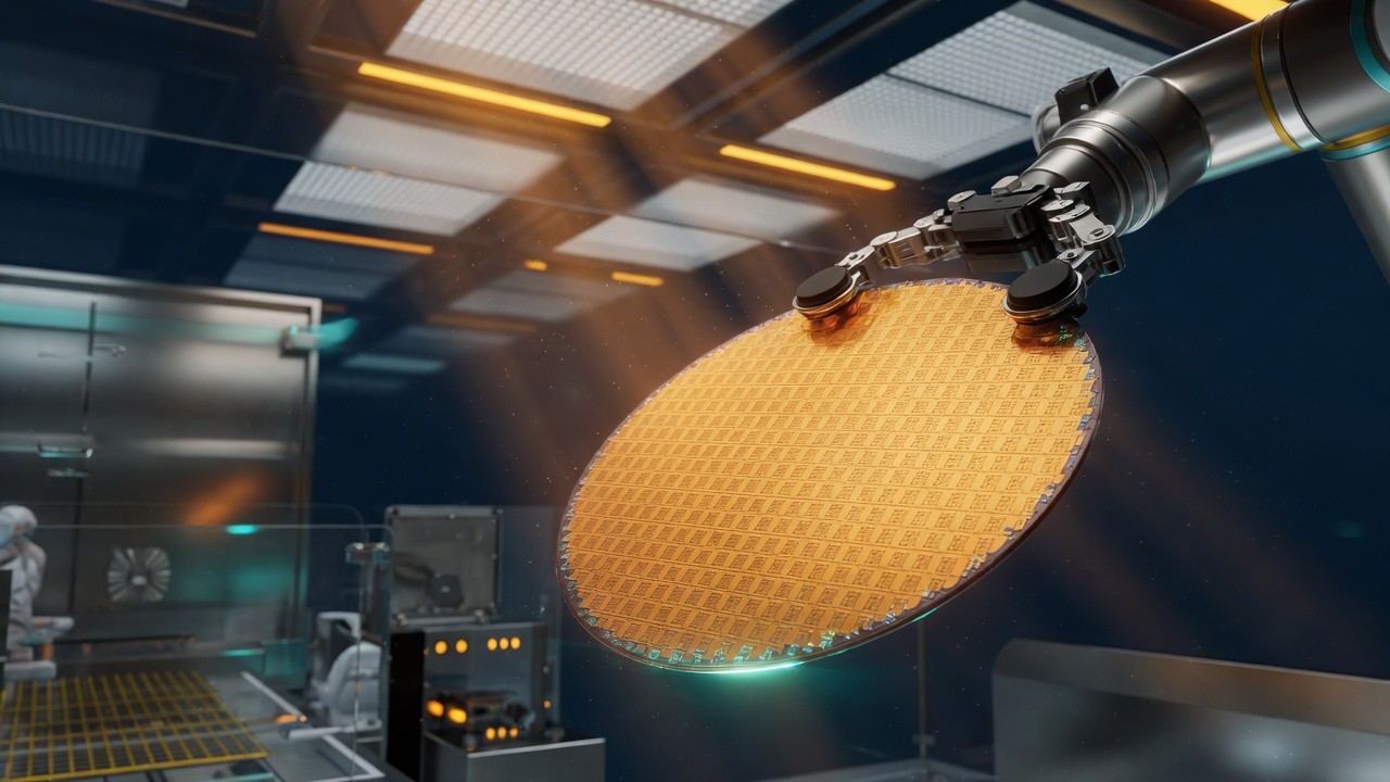
India is building its first semiconductor fabs. I've been tracking every project for the past two years, and the pace of announcements has gone from "one big headline a quarter" to "something new every week." Here's every project, where it stands, and what it means for hiring.
I'll keep this updated as things change. Bookmark it.
Tata Electronics Dholera Fab (Gujarat)
This is the big one. India's first proper semiconductor fabrication plant.
- Investment: $11 billion (about Rs 91,000 crore)
- Location: Dholera Special Investment Region, Gujarat
- Partner: PSMC (Powerchip Semiconductor Manufacturing Corporation), Taiwan
- Technology: Starting at 28nm, with plans to move to more advanced nodes
- Timeline: Construction ongoing. First silicon expected late 2026 or early 2027.
- Jobs: 20,000+ direct jobs once fully operational. Thousands more during construction and in the supply chain.
28nm sounds old if you're used to reading about TSMC's 3nm. But 28nm is a sweet spot. It covers automotive chips, IoT, industrial controllers, display drivers, and a huge chunk of the analog/mixed-signal market. The global demand for 28nm and above is massive and growing. This is a smart starting point.
PSMC brings the process knowledge. Tata brings the capital and local execution capability. The Indian government is subsidizing roughly 50% of the capital cost through the India Semiconductor Mission.
Tata OSAT Plant, Jagiroad (Assam)
This one is actually closer to production than the Dholera fab.
- Investment: Rs 27,000 crore ($3.26 billion)
- Location: Jagiroad, Morigaon district, Assam
- Type: OSAT (Outsourced Semiconductor Assembly and Test)
- Commissioning: April 2026. Yes, this month.
- Capacity: 48 million chips per day at full production
- Jobs: 15,000 direct jobs
OSAT is where chips get packaged and tested after fabrication. This is not chip design or wafer manufacturing. But it's a genuine semiconductor manufacturing operation. The skills needed are different from design: process engineering, equipment maintenance, quality control, yield analysis, supply chain management.
48 million chips per day is serious volume. For context, that's in the same ballpark as mid-sized OSAT facilities in Malaysia and Vietnam that currently handle packaging for global chipmakers.
Kaynes Semicon (Sanand, Gujarat)
- Investment: Rs 3,307 crore
- Location: Sanand, Gujarat
- Type: OSAT
- Status: Inaugurated March 2026
- Focus: Automotive and industrial semiconductors
Kaynes is an Indian electronics manufacturing company that's been around since 2008. Their entry into OSAT is significant because it's not a Tata-scale mega-project. It's a mid-size, focused operation targeting the automotive semiconductor supply chain. With India's auto industry booming and automotive chip shortages still fresh in everyone's memory, this makes commercial sense.
Intel-Tata Partnership
- Investment: $14 billion combined
- Status: MoU signed, details still emerging
- Scope: Advanced packaging and potentially chip fabrication
This partnership was announced with a lot of fanfare. The $14B number is eye-catching. But specifics on what gets built where and when are still thin. Intel has been reorganising its own foundry business globally, so the timeline here could shift. I'd keep expectations moderate until we see ground broken.
That said, Intel already has a large design center in Bangalore with 10,000+ engineers. Any manufacturing partnership would leverage that existing talent base. Intel is one of the top semiconductor employers in India.
Indo-Taiwan Industrial Park (Sanand-Dholera)
- Announced: April 2026
- Location: Between Sanand and Dholera, Gujarat
- Concept: Dedicated industrial zone for Taiwanese semiconductor and electronics companies
This is the newest announcement. The idea is to create a cluster effect. Instead of isolated fabs, you build an ecosystem: the fab, the OSAT facility, the equipment suppliers, the chemical suppliers, the testing houses, all within driving distance of each other. Taiwan's Hsinchu Science Park works exactly like this, and it's one reason Taiwan dominates chip manufacturing. SEMI, the global industry association, has noted that cluster-based development is the most effective model for building semiconductor ecosystems.
Gujarat is clearly positioning itself as India's semiconductor hub. Dholera fab + Sanand OSAT + this industrial park = the beginnings of a real cluster.
What this means for jobs
Here's what I think people get wrong: they hear "semiconductor fab" and think "chip design jobs." That's not what fabs create. Fabs create manufacturing jobs.
The job categories that will see the biggest hiring from these projects:
Manufacturing and process engineering
- Process engineers (thin film, etch, lithography, CMP, implant)
- Equipment engineers (maintaining ASML, Applied Materials, Lam Research tools)
- Yield engineers (analyzing defects, improving yield from 60% to 90%+)
- Process integration engineers (making the whole flow work together)
Packaging and test
- Package design engineers
- Test engineers (ATE programming, test flow development)
- Failure analysis engineers
- Reliability engineers
Support functions
- Supply chain and procurement (chemicals, gases, wafers, equipment parts)
- Quality engineers (ISO, IATF for automotive)
- EHS (Environment, Health, Safety) - fabs use hazardous chemicals
- Facilities engineers (cleanroom HVAC, ultra-pure water systems, gas delivery)
Chip design jobs will grow too, but indirectly. As India builds manufacturing capability, more design houses will set up or expand in India. The ecosystem feeds itself.
Skills needed: fab vs design roles
If you're an ECE or VLSI engineer thinking about fab roles vs design roles, here's the honest comparison:
| Fab/Manufacturing Roles | Design Roles | |
|---|---|---|
| Education | B.Tech/M.Tech in ECE, Material Science, Chemical Engineering, Physics | B.Tech/M.Tech in ECE, EEE |
| Key skills | Semiconductor physics, cleanroom processes, SPC, equipment operation | Verilog/VHDL, EDA tools, digital/analog design |
| Work environment | Cleanroom (bunny suits, shift work common) | Office/WFH |
| Starting salary | 8-15 LPA (estimated for India fabs) | 4-30 LPA (wide range, service to product) |
| Location | Must be at the fab site | Bangalore, Hyderabad, Noida, Pune |
Fab roles are less flexible on location and often involve shift work. But they're also more hands-on, and there's something deeply satisfying about being part of the physical creation of a chip rather than just the digital representation of one.
Should you wait for fab jobs?
No. Don't put your career on hold waiting for the Dholera fab to start hiring. Get into the industry now through design roles, service companies, or OSAT roles at Jagiroad/Sanand. Our fresher's roadmap to landing a VLSI job covers exactly how to do this. When the fabs ramp, experienced semiconductor professionals will be first in line for leadership positions.
The people who will benefit most from India's fab buildout are those who are already in the semiconductor industry when these facilities start production. Start now. Check the latest semiconductor job openings and get your foot in the door.
Related reading
Frequently asked questions
When will India's first semiconductor fab start production?
The Tata-PSMC Dholera fab in Gujarat is targeting first silicon in late 2026 or early 2027, starting at 28nm technology. Full production ramp will take another 12-18 months after that. The Tata OSAT plant in Assam is commissioning in April 2026 and will be operational sooner since packaging is less complex than wafer fabrication.
How many jobs will India's semiconductor fabs create?
Direct jobs: 20,000+ at Dholera fab, 15,000 at Tata OSAT Assam, and several thousand at Kaynes Sanand. Including indirect jobs (supply chain, equipment servicing, logistics), estimates range from 50,000-100,000 new semiconductor-related positions by 2028. These span engineering, technician, operations, and management roles.
What qualifications do I need for semiconductor fab jobs in India?
B.Tech or M.Tech in ECE, Material Science, Chemical Engineering, or Physics. Fab roles value semiconductor physics, cleanroom process knowledge, and statistical process control. Unlike design roles that need EDA tool expertise, fab roles need hands-on understanding of deposition, etching, lithography, and metrology equipment.
Which Indian state is leading in semiconductor manufacturing?
Gujarat is leading with three major projects: the $11B Tata-PSMC fab at Dholera, Kaynes OSAT at Sanand, and the upcoming Indo-Taiwan Industrial Park between Sanand and Dholera. Assam follows with the Rs 27,000 crore Tata OSAT plant at Jagiroad. Gujarat's cluster approach mirrors Taiwan's Hsinchu Science Park model.
Will India's fabs compete with TSMC and Samsung?
Not directly, and that's by design. India's fabs start at 28nm, while TSMC and Samsung are at 3nm and below. India is targeting the mature-node market: automotive, IoT, industrial chips. This market is huge and growing, with global 28nm+ capacity consistently sold out. India doesn't need to beat TSMC to succeed commercially.