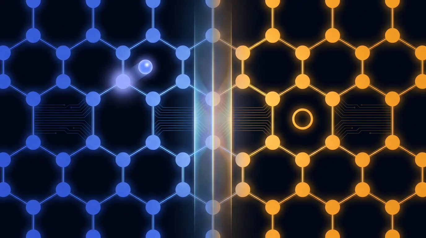
Pure silicon is a mediocre conductor
On its own, silicon is a bit of a letdown. Every atom uses all four of its outer electrons to bond with four neighbours, so the lattice is a party where every guest's hands are full — nothing is free to move, and the crystal barely conducts. Useful as a starting point, useless as a device.
The industry's masterstroke is doping: deliberately sprinkling in a trace of a foreign element — roughly one atom in a million — chosen for having exactly one bonding electron too many, or one too few. That tiny, precisely placed impurity is what turns inert silicon into the working material of every chip.
Two flavours: N-type and P-type
Pick a dopant one column to the right of silicon in the periodic table — phosphorus — and it arrives with five bonding electrons. Four slot neatly into the lattice; the fifth has no bond to join, so it roams free. That spare, mobile electron is a negative carrier, and silicon doped this way is N-type (N for negative).
Pick a dopant one column to the left — boron — and it brings only three bonding electrons. That leaves a vacancy in the bonding network, a hole. Neighbouring electrons shuffle in to fill it, which makes the hole itself appear to drift through the crystal like a positive charge. Silicon doped this way is P-type (P for positive). Toggle between them below.
Phosphorus brings five bonding electrons; four join the lattice and the fifth roams free — a mobile negative carrier.
Two points worth holding onto. First, neither material is actually charged overall — the names describe who does the moving, not a net charge. Second, the reason a sprinkle of dopant matters so much is that pure silicon starts with almost no free carriers, so even a few added ones dominate. The idea of the free electron and the hole comes straight from the band gap: a carrier above, a hole below.
You dope silicon with boron, which has three bonding electrons to silicon's four. What did you just make?
Press them together: the junction
Doping's real power shows up when you put the two flavours side by side. Press a slab of N against a slab of P and something remarkable happens at the boundary. Free electrons from the N side and holes from the P side meet and cancel near the join, leaving a thin depletion region that acts like a built-in gate.
The result is a diode: current can cross the junction easily in one direction but is blocked in the other — a one-way valve for electricity. Select Diode in the figure above to watch current pass one way only. Diodes alone are everywhere — in chargers, radios, and every device that converts alternating current to direct — but they're also the stepping stone to something bigger.
Sandwich them: the transistor
Now make a sandwich: N-P-N, two outer regions of one flavour around a thin middle layer of the other. That thin middle layer becomes a control gate. Apply a small voltage to it and it opens a conducting channel between the two outer regions, letting current flow. Remove the voltage and the channel closes. Select Transistor above and toggle the gate to feel it.
That controllable sandwich is a transistor — the exact switch that all of computing rests on. It is the physical realisation of the door: a small control signal decides whether current flows or not, flipping between on and off billions of times a second. Doping is what makes it buildable, because it gives engineers the two flavours of silicon the sandwich requires.
In an N-P-N transistor, what does a small voltage applied to the thin middle (P) layer do?
Why this scales to billions
The last piece is that doping is patternable. Using lithography, engineers define exactly where the N and P regions go, down to a few atoms wide, and repeat the pattern across a wafer. A modern chip is billions of these doped sandwiches — transistors — wired together with fine metal lines. The same trick that made one switch makes a trillion.
Step back and the whole industry snaps into focus: refine sand into flawless silicon, dope it into N and P, stack those into transistors, wire the transistors into logic, and wire the logic into chips. Every layer rests on the one below — and doping is the layer that turns a passive crystal into an active switch.
Key takeaways
- Pure silicon barely conducts — every electron is bonded. Doping adds ~one foreign atom per million to control its carriers.
- N-type (phosphorus, a spare electron) carries negative charge; P-type (boron, a hole) carries positive charge. Neither is net-charged — the names say who moves.
- Press N against P for a diode — a one-way valve with a built-in depletion region.
- Sandwich N-P-N and the thin middle layer gates the channel — a transistor, the switch every chip is built from, patternable by the billion.
Frequently asked questions
What is doping in semiconductors?
Doping is deliberately adding a trace of a foreign element to pure silicon — roughly one dopant atom per million silicon atoms — to control how it conducts. Pure silicon has all its electrons locked in bonds, so it barely conducts. A dopant with one extra bonding electron (like phosphorus) adds free electrons; a dopant with one fewer (like boron) creates holes. This tiny, precisely placed impurity is what turns inert silicon into the working material of every chip.
What is the difference between N-type and P-type silicon?
They differ in which charge carrier does the work. N-type silicon is doped with an element like phosphorus that has five bonding electrons; four join the lattice and the fifth roams free, giving negative carriers — hence 'N'. P-type silicon is doped with an element like boron that has only three bonding electrons, leaving a vacancy called a hole; neighbouring electrons hop into it, so the hole drifts like a positive carrier — hence 'P'. Neither material carries a net charge overall; the letters just name who moves.
How does doping create a transistor?
By stacking doped regions. Put an N-type region against a P-type region and you get a diode: current crosses the junction in only one direction. Make a sandwich — N-P-N — and the thin middle layer becomes a control gate. A small voltage on that middle layer opens or closes the conducting channel between the two outer regions, switching current on and off. That controllable sandwich is a transistor, the switch at the heart of every chip.
What elements are used to dope silicon?
The two classic dopants are phosphorus (and sometimes arsenic or antimony) for N-type, because they sit one column to the right of silicon in the periodic table and bring an extra bonding electron; and boron for P-type, because it sits one column to the left and is short one electron. Only a trace is needed — about one dopant atom per million to per hundred-million silicon atoms — and it's introduced by diffusion or ion implantation, then patterned with lithography.
Why does adding just one atom in a million change silicon so much?
Because pure silicon has almost no free carriers to begin with, so even a tiny number of added carriers dominates its behaviour. Each phosphorus atom contributes one free electron; sprinkle in one per million silicon atoms and you've added an enormous number of carriers compared to the near-zero baseline — enough to raise conductivity by orders of magnitude. The effect is huge precisely because you're adding to almost nothing, and because the dopant sits neatly in the crystal without disrupting it.
See how you’d score in a real interview.
These deep dives build the foundation. The readiness check goes further: questions drawn from real semiconductor interviews, scored instantly, with a clear read on where you stand and what to work on next.
Take the free readiness checkFree, from semiconductor.cv — the career platform behind this series.
Preparing for semiconductor interviews? Take the free readiness check →